P N Junction Circuit Diagram
Download P N Junction Circuit Diagram Pics. 30 840 просмотров 30 тыс. In forward bias, resistance of diode, rd =0 or it acts as a short circuit and output voltage equals the input voltage.
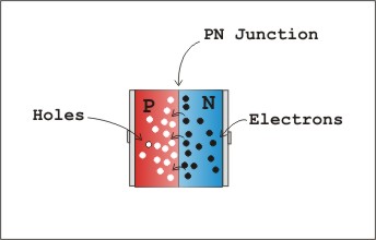
A pn junction is a structure formed by neighboring regions, with different dopings.
Diode function the main function of the semiconductor diode is the … A zener diode when reverse biased can either undergo avalanche break down or. Connect the circuit as shown in figure (1) using silicon pn junction diode. Note that this does not automatically align.

0 Response to "P N Junction Circuit Diagram"
Post a Comment